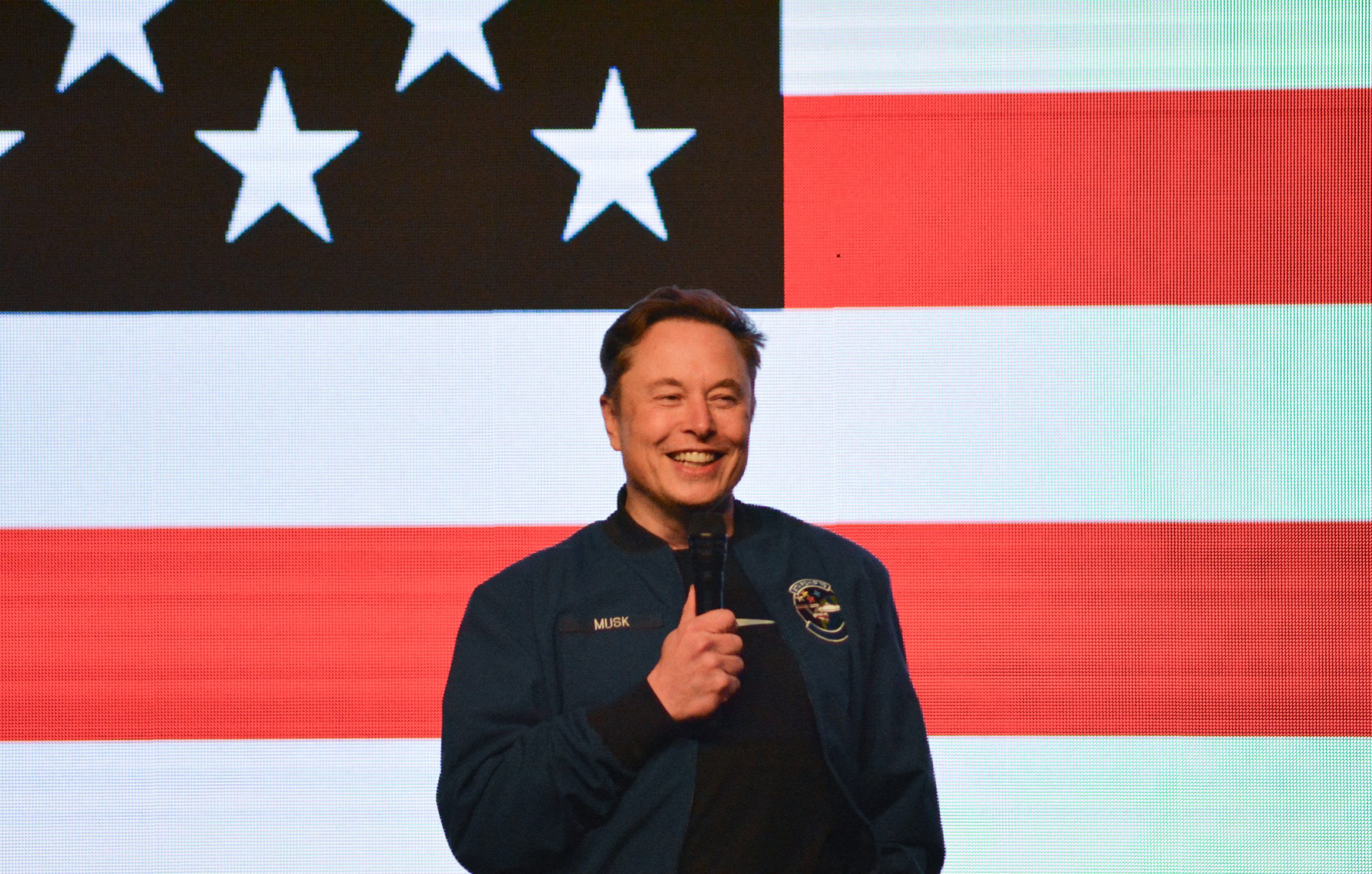
In a significant strategic move, entrepreneur Elon Musk has revealed an ambitious initiative to establish a dedicated chip-building facility, dubbed "Terafab," through a collaborative effort between his key companies, Tesla and SpaceX, with an implicit role for his artificial intelligence venture, xAI. This bold undertaking signals a profound shift towards vertical integration, aiming to secure a proprietary supply of advanced semiconductors crucial for the escalating demands of artificial intelligence and robotics across his diverse portfolio.
Musk publicly articulated these plans at a recent event in downtown Austin, Texas, sharing visual concepts that suggest the "Terafab" facility would be strategically located near Tesla’s existing Austin headquarters and its expansive "gigafactory." The proposed proximity could facilitate seamless logistical integration and foster synergy between design, manufacturing, and application.
The Genesis of "Terafab": A Response to Growing Demands
The driving force behind this colossal endeavor, according to Musk, stems from a perceived bottleneck in the global semiconductor supply chain. He contends that current external manufacturers are unable to produce chips at the necessary speed and scale required to keep pace with the exponential growth of artificial intelligence and robotics technologies integral to his ventures. "We either build the Terafab or we don’t have the chips, and we need the chips, so we build the Terafab," Musk stated, underscoring the perceived urgency and strategic imperative of the project.
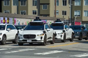
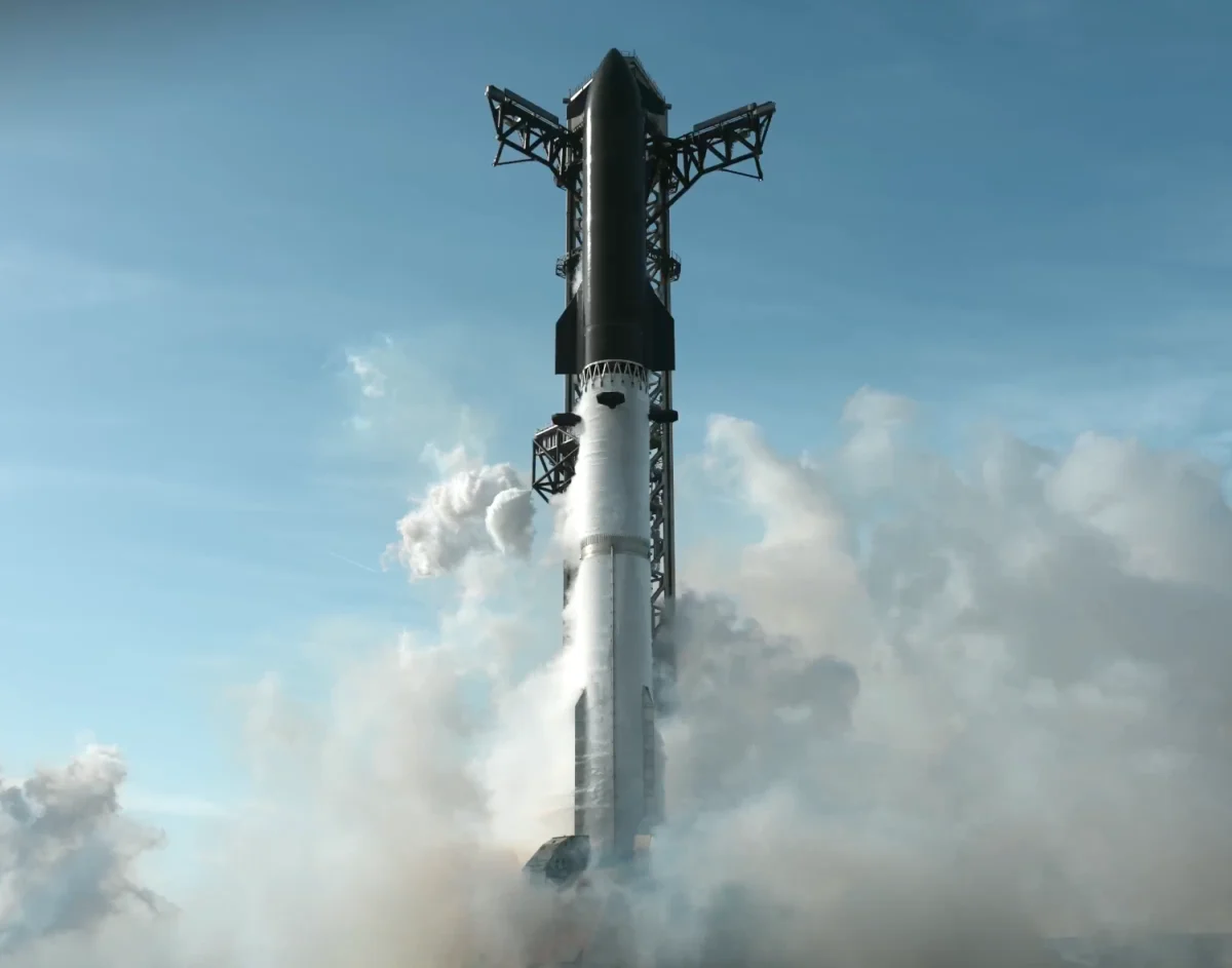
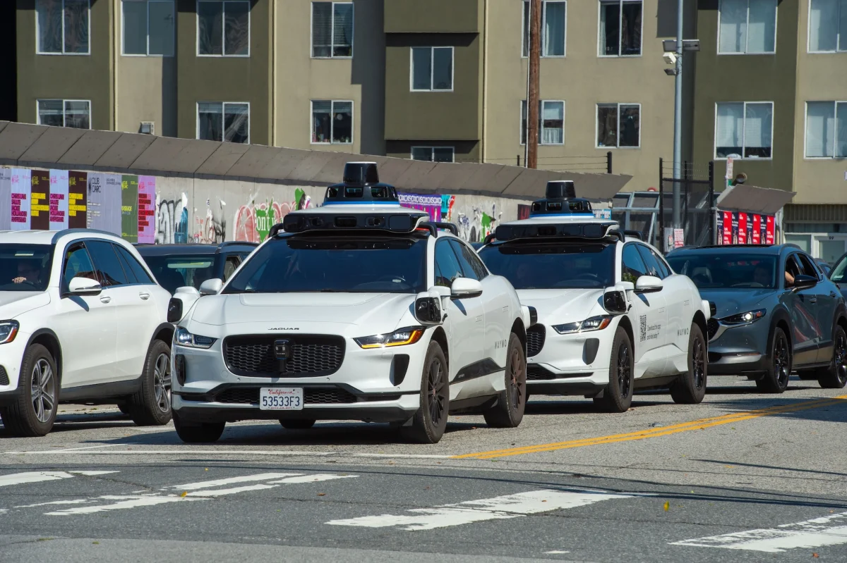
This declaration is not merely a statement of intent but a direct response to the insatiable computational appetite of his companies. Tesla’s aspirations for fully autonomous driving, powered by increasingly sophisticated neural networks, demand unparalleled processing capabilities. SpaceX’s Starlink satellite constellation, with its millions of active terminals and planned expansion, requires robust, efficient, and custom-designed silicon for orbital and ground-based operations. Furthermore, xAI, Musk’s recently launched artificial intelligence company, aims to develop advanced AI models that will require vast arrays of specialized chips for training and inference, potentially rivaling the most powerful supercomputers on Earth.
The stated objectives for the Terafab facility are monumental: to manufacture chips capable of supporting an astounding 100 to 200 gigawatts of computing power annually for terrestrial applications, alongside an even more ambitious target of one terawatt of computing power in space. While a specific timeline for these audacious plans was not provided, the scale of the ambition alone speaks volumes about Musk’s long-term vision for technological independence.
Tesla’s Prior Forays into Custom Silicon
This latest announcement from Musk is not entirely without precedent within his corporate ecosystem. Tesla, in particular, has a well-documented history of moving towards in-house silicon development to gain a competitive edge and reduce reliance on external suppliers.
Historically, early Tesla vehicles relied on graphics processing units (GPUs) from NVIDIA for their Autopilot system. However, in 2019, Tesla made a pivotal decision to transition away from third-party hardware, unveiling its custom-designed Full Self-Driving (FSD) computer. Developed under the leadership of Pete Bannon, formerly of Apple, this system-on-a-chip (SoC) demonstrated Tesla’s capacity to engineer complex, high-performance silicon tailored specifically for its automotive AI needs. This move allowed Tesla greater control over the hardware-software stack, optimizing performance, power efficiency, and cost.
Building on this foundation, Tesla further pushed the boundaries of in-house silicon with the development of its D1 chip, the core component of its Dojo supercomputer. Dojo is designed for the intensive training of AI models, particularly those underpinning Tesla’s autonomous driving systems. The D1 chip, a 7-nanometer processor, is engineered for massive parallelism and high bandwidth, enabling rapid iteration and improvement of AI algorithms. The existence and ongoing development of Dojo represent a significant investment in specialized AI hardware, laying some groundwork for the expertise and infrastructure that might be leveraged for the Terafab project. While Dojo focuses on AI training chips, the Terafab implies a broader scope, potentially encompassing a wider array of custom chips for various applications across Tesla, SpaceX, and xAI.
The Immense Challenges of Semiconductor Manufacturing
While Musk’s track record includes the successful realization of projects once deemed impossible, such as reusable rockets and the mass production of electric vehicles, venturing into semiconductor manufacturing presents a unique set of colossal challenges. The chip industry is arguably one of the most capital-intensive, technologically complex, and talent-dependent sectors globally.
Establishing a modern semiconductor fabrication plant, or "fab," typically requires investments ranging from $10 billion to $20 billion, with some advanced facilities exceeding $30 billion. This capital expenditure covers everything from ultra-clean rooms and highly specialized machinery (like extreme ultraviolet lithography machines, which can cost hundreds of millions of dollars each) to intricate material handling systems.
Beyond the financial outlay, the technical hurdles are immense. Semiconductor manufacturing involves hundreds of intricate steps, each requiring picometer-level precision. Achieving high yield rates—the percentage of functional chips produced from a silicon wafer—is a continuous battle, even for seasoned industry veterans like TSMC, Samsung, and Intel, who have decades of accumulated knowledge and experience. The processes are highly sensitive to contamination, temperature fluctuations, and vibrations, demanding an unprecedented level of environmental control.
Furthermore, the talent pool for semiconductor engineers, process experts, and equipment specialists is highly specialized and fiercely competitive. Attracting and retaining such expertise would be crucial for the success of Terafab, potentially necessitating a significant recruitment drive from established chip-making hubs. Musk’s lack of a direct background in semiconductor manufacturing, as noted by observers, adds another layer of scrutiny to this ambitious undertaking.
Strategic Implications and Market Impact
Should the Terafab initiative come to fruition, its strategic implications for Musk’s companies and the broader technology landscape could be profound. For Tesla, SpaceX, and xAI, it promises an unparalleled degree of control over their hardware supply chain, ensuring access to custom-designed, high-performance chips optimized for their specific applications. This vertical integration could reduce dependencies on external geopolitical factors, such as trade disputes or regional conflicts, which have repeatedly disrupted global chip supplies in recent years. It could also accelerate innovation by allowing tighter integration between chip design, software, and end-product development.
The broader market impact, however, is more speculative. The existing foundry market is dominated by a few giants like TSMC (Taiwan Semiconductor Manufacturing Company) and Samsung Foundry. While a new player, especially one backed by Musk’s resources, could introduce competition, the sheer scale required to rival these established players is staggering. Terafab would likely initially focus on highly specialized chips for internal consumption rather than attempting to become a general-purpose foundry. Nevertheless, if successful, it could signal a trend where other large tech companies, facing similar supply constraints and desires for customization, might consider their own fab ventures, albeit a challenging prospect.
Culturally, the concept of a "terawatt in space" for computing power is particularly captivating. It evokes visions of massive orbital data centers, advanced space-based AI, and unprecedented computational capabilities for future interplanetary missions or off-world colonization efforts. Such a development could fundamentally alter the economics and feasibility of deep-space exploration and resource utilization.
Austin’s Expanding Tech Footprint
The proposed location of Terafab in Austin further solidifies the city’s burgeoning status as a major technology and manufacturing hub. Austin has already attracted significant investments from tech giants, including Tesla’s Gigafactory Texas and headquarters, Samsung’s large chip manufacturing plant, and expansions by Apple, Google, and Amazon. The addition of Terafab would not only create numerous high-skilled jobs but also contribute to a deepening ecosystem of semiconductor expertise and infrastructure in the region. This concentration of talent and resources could foster further innovation and attract ancillary businesses, transforming Austin into an even more critical node in the global tech supply chain.
Looking Ahead: Ambition Versus Execution
Elon Musk’s ventures are frequently characterized by audacious goals and ambitious timelines, often encountering initial skepticism before eventually achieving significant breakthroughs. His history, as noted by various commentators, includes instances of overpromising on timelines and deliverables. The Terafab project, with its immense technical and financial demands, fits squarely into this pattern.
The transition from conceptualization to full-scale, high-yield production in semiconductor manufacturing is a journey fraught with technical complexities, unforeseen delays, and colossal capital requirements. While Tesla’s past success with custom FSD chips and the D1 for Dojo demonstrates a foundational capability in chip design, operating a full-fledged fabrication plant is an entirely different magnitude of challenge.
The ultimate success of Terafab will hinge on Musk’s ability to assemble a world-class team of semiconductor veterans, secure vast funding, and navigate the intricate technological landscape of chip manufacturing. It represents a quintessential Muskian gamble: a high-risk, high-reward endeavor that, if successful, could redefine the strategic independence of his companies and potentially reshape aspects of the global technology industry. As the world watches, the journey from announcement to operational reality for Terafab will undoubtedly be one of the most compelling narratives in the coming years.


